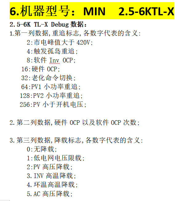
MIN series History data meaning
MIN 2.5-6KTL-X
1. MODEL Number:
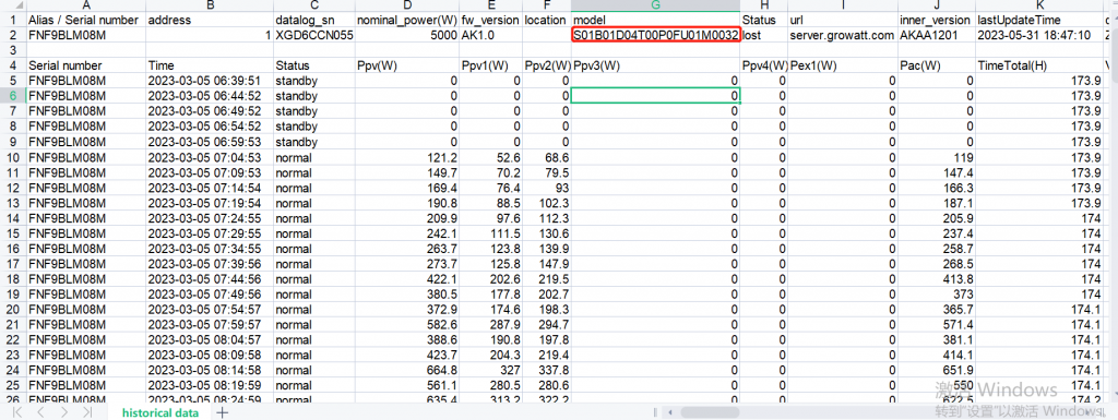
S01B01D04T00P0FU01M0032
S:Safety 0-26
B: Function1
D:Display ODM manufacturer
T: Function 2
P:Function3
U:Environment, Machine working environment, AC voltage range, PV ground
M:Power power section, accuracy is 100W
Safety
S00: Null
S01: VDE0126
S02: G99
S03: AS4777_Australia
S04: CEI0_21
S05: cS_SP1663
S06: reserved Xila
S07: N4105 (include VDE4105 and France)
S08: G98
S09: EN50438(Ireland)
S0A: CQC
S0B: EN50438 default(Include Switzerland, Poland, Turkey,Greece,VgridAvg10min>253V protection)
S0C: Hungary–>IEC62717&IEC62116
S0D: Belgium
S0E: MEA
S0F: PEA
S10: AS4777_Newzealand
S11: CQC_Plant
S12: India
S13: EN50438_Demark
S14: EN50438_Sweden
S15: EN50438_Norway
S16: cS_Queensland
S17: France_VFR2014
S18: cS_Korea60Hz
S19: Brazil
S1A: CEI0-16
S1B: Dewa
S1C: cS_Chile
S1D cS_Argentina
S1E: BDEW
S1F: cS_TAIWAN
S20: cS_TR3_2_1_Demark (for PV INV)
S21: CQC2018
S22: cS_TR3_3_1_Demark (for storage INV)
B: Function1
Bit0-Bit1 Exporting current limitation Enable
0: Disable exportLimit;
1: Enable 485 exportLimit;
2: Enable 232 exportLimit;
3: Enable CT exportLimit
Bit2 APF/SVG Enable
1: Enable APF/SVG
0:Disable APF/SVG
Bit3 AFCI Enable
1: Enable AFCI
0:Disable AFCI
Bit4 Battery type
0:lead acid battery
1:lithium-ion battery
Bit5 Battery type
APF/SVG Disable/Enable
1: Enable APF/SVG
0:Disable APF/SVG
Bit6-Bit7
Reserved
D:Display ODM
PV Inverter 0
Growatt Inverter 1
InterlBras 2
正泰/CHNT 3
通用机型 4
Sunrun 5
Rihome 6
T Function
Bit0 PID Enable
0: Disable
1: Enable
Bit1 PV string Monitoring Enable
0: Disable
1: Enable
Bit2 Selection of fan speed regulation scheme
0: Normal Fan speed regulation Solution
1: Selection of fan speed regulation and mute solution
Bit3 Select Relay Solution
0: Disable
1: Enable
Bit4 AC SPD detection function enable
0: Disable
1: Enable
Bit5 DC SPD detection function enable
0: Disable
1: Enable
Bit6 custom logo (for non-universal function selection)
Bit7 Reserved
P Function
Bit0 ISO Enable
0: Disable
1: Enable
Bit1 DCI Enable
0: Disable
1: Enable
Bit2 GFCI Enable
0: Disable
1: Enable
Bit3 Customer Protection range custom enable
0: Disable
1: Enable
Bit4-Bit7 Reserved
U(Environment)
Bit0-Bit2 Grid Volt
0:277V
1:230V
2:288V
3:127V
4、462V
5、208V
Bit3 PV Negative is connected to ground Enable
0:Disable
1:Enable
Bit4-Bit7 Reserved
M:Power Power Section, Accuracy Is 100W
2.5 Power segment
Accuracy is 100W ,like 80K is 0x320 , that’s 0x0320

2. Firmware Version
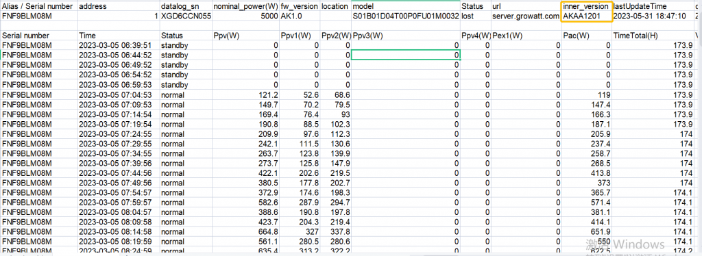
3. Status
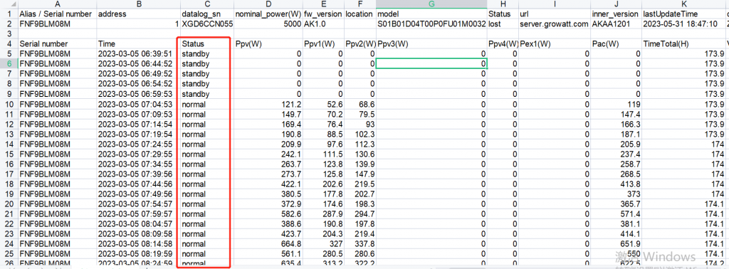
Standby
Waiting
Normal
Fault
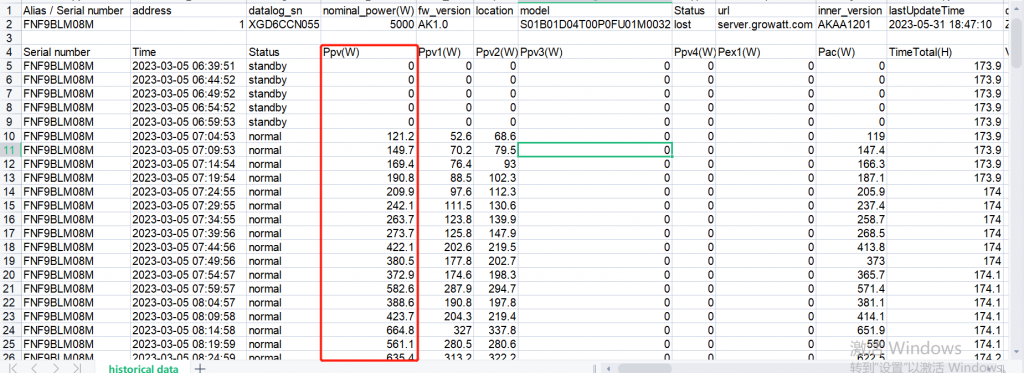
4. Ppv(w) Total PV power
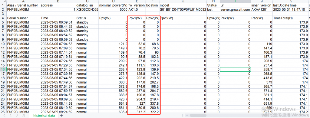
5. Ppv1, Ppv2(w) MPPT power
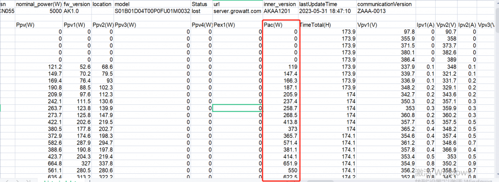
6. Pac(w)
7. 2 MPPT voltage, Current
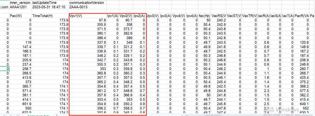
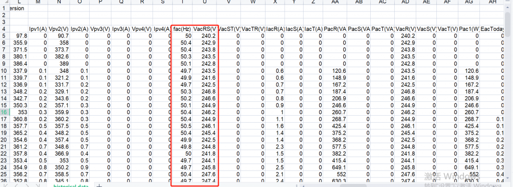
8. Fac, Vac (Grid voltage, frequency)
9. IVN_Temp
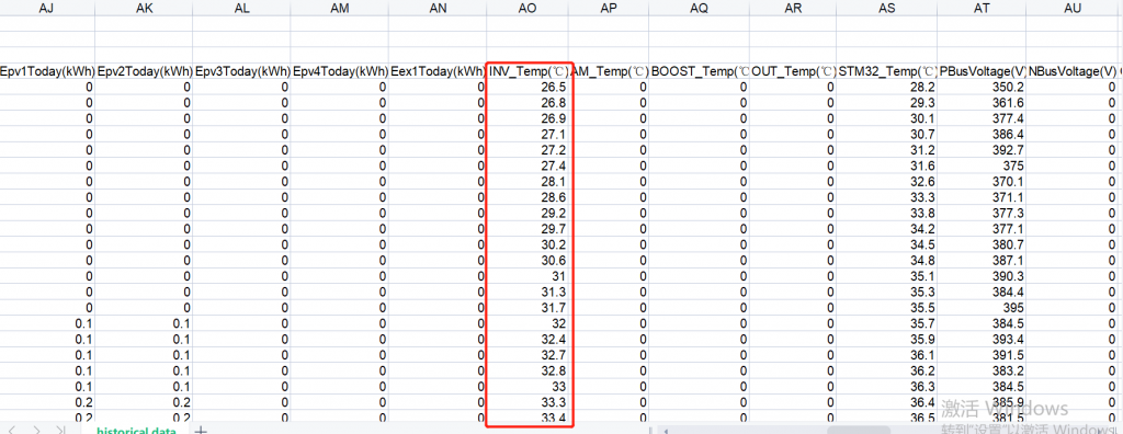
Temperature sensor is designed on DC-AC circuit on mainboard
10. STM32_Temp
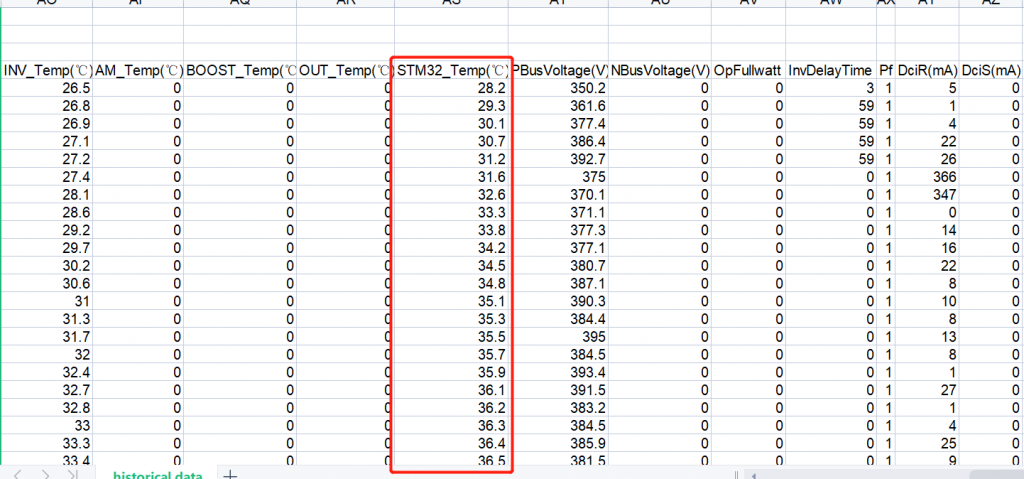
M3 board temperature
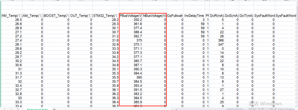
11. PBusVoltage, NBusVoltage
12. OpFullwatt
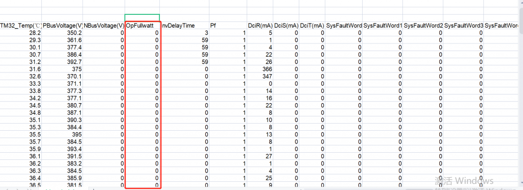
Output Power limit value
13. nvDelay Time
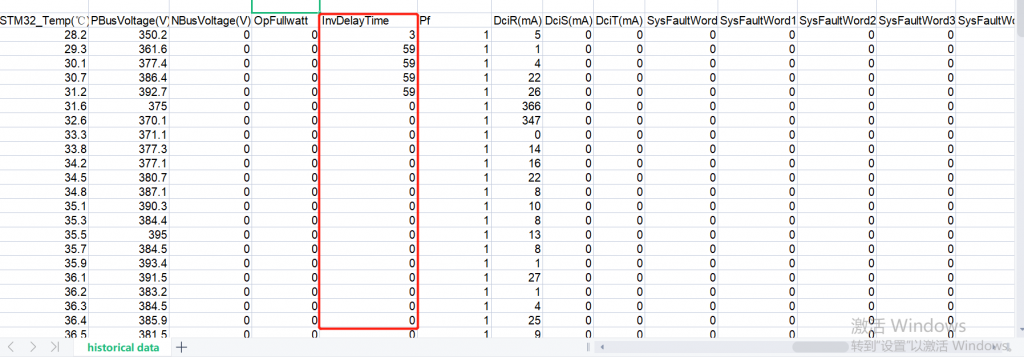
The countdown time that connect to grid
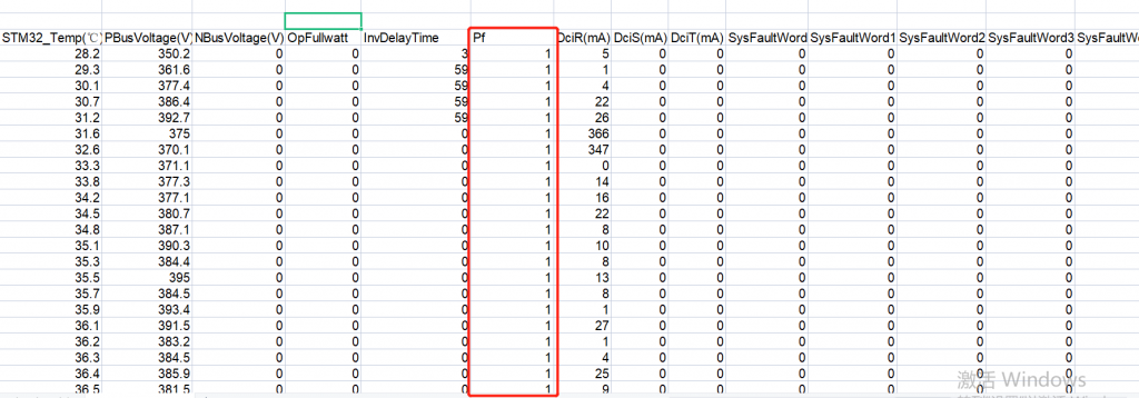
14. PF
15. DCI
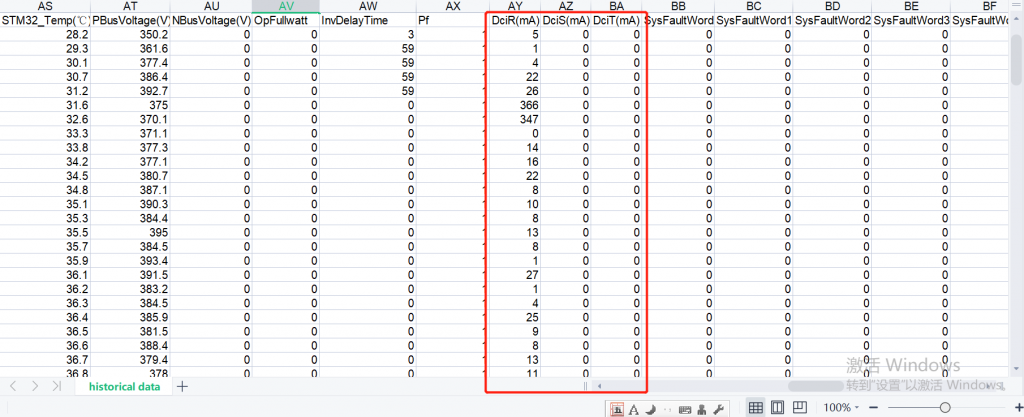
16. AFCI
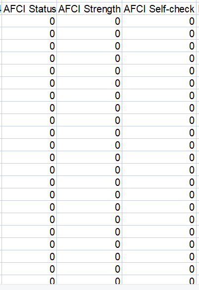
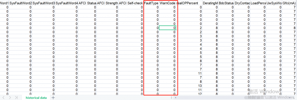
17. FaultType
18. realOPPercent
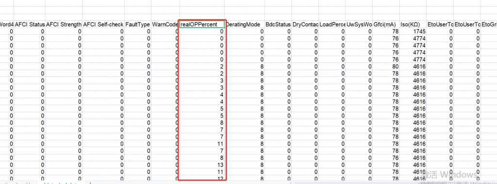
Real Power / Total Power
19. Derating Mode
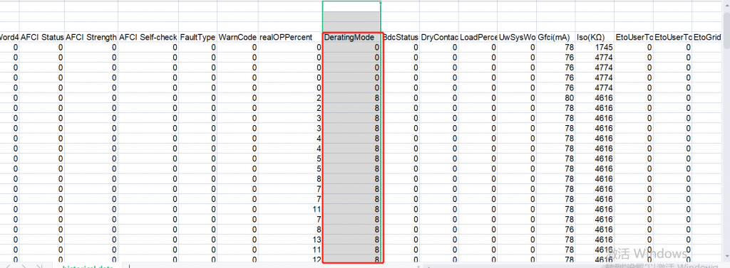
Please read 22th row about Debug1, degrating mode has been introduced there
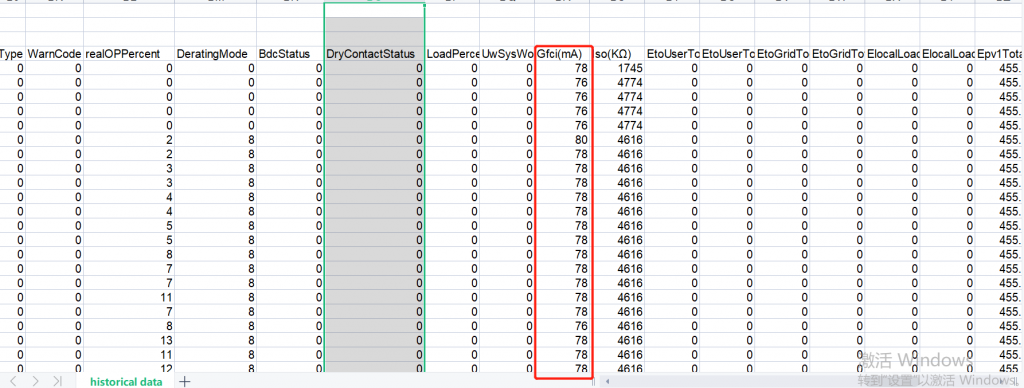
20. GFCI
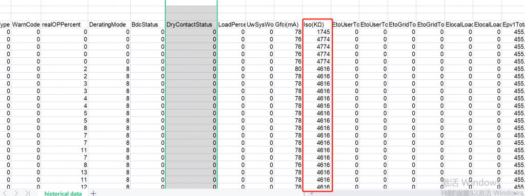
21. ISO
22. Debug1
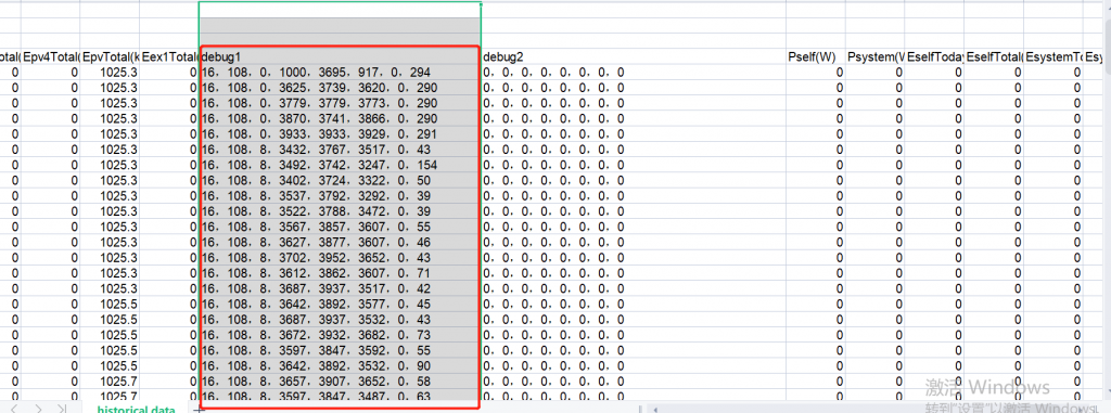
debug1:
For example:
16,108,0,1000,3695,917,0,294
First register address meaning
2: Grid peak voltage is greater than 420V
4. trigger island retake
8. Software Inv OCP
16. Hardware OCP
32. Aging Command Toggle
64. PV1 low power recovery
128. PV2 low power recovery
256. PV is lower than start voltage
Second register address meaning
Count of Hardware and software OCP
Third register address meaning
Degrading mode
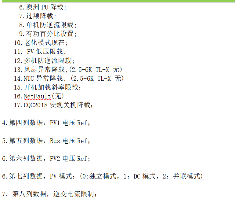
0:
No Degrading
1:
Low grid voltage limit AC output
2:
PV high voltage degrade
3:
INV High Temperature degrade
4:
Ambient temperature high temperature derating
5:
AC High Voltage Degrade
6:
Australia PU Degrade
7:
Over Frequency Degrade
8:
Single inverter Exporting Current limitation Degrade
9:
Active energy percentage setting
10:
Aging mode now Degrade
11:
PV low Voltage Degrade
12:
Multi inverters exporting current limitation Degradeing
13
Fan Abnormal Degrade( 2.5-6KTL-X None )
14
NTC Abnormal Degrade( 2.5-6KTL-X None )
15
Power-on load slope limit
16
NetFault( None)
17
CQC2018 Safety Type Power off Degrade
Fourth register address meaning
PV1 Voltage Ref
Fifth Register Address Meaning
Bus Voltage Ref
6th Register Address Meaning
PV2 Voltage Ref
7th Register Address Meaning
PV mode ( 0: Independent, 1: DC mode, 2. In parallel
8th Register Address Meaning
INV Current Limit
