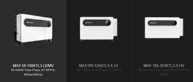
MAX 50K-80K TL3 introduction
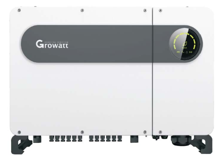
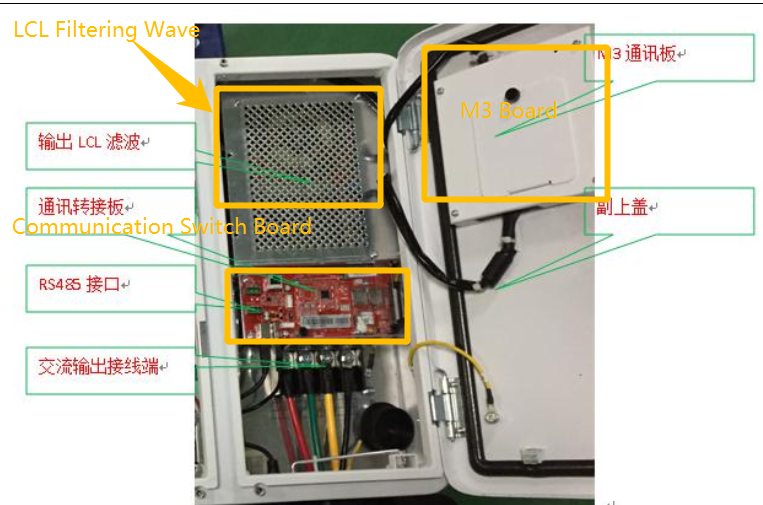
1. Product appearance
MAX LV model and MAX MV model have same boards
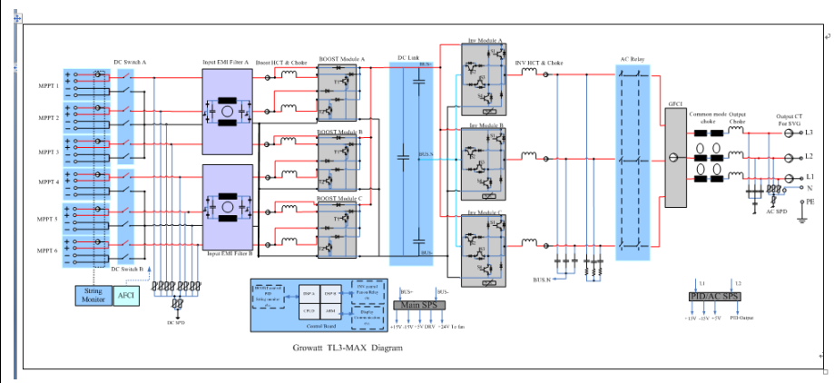
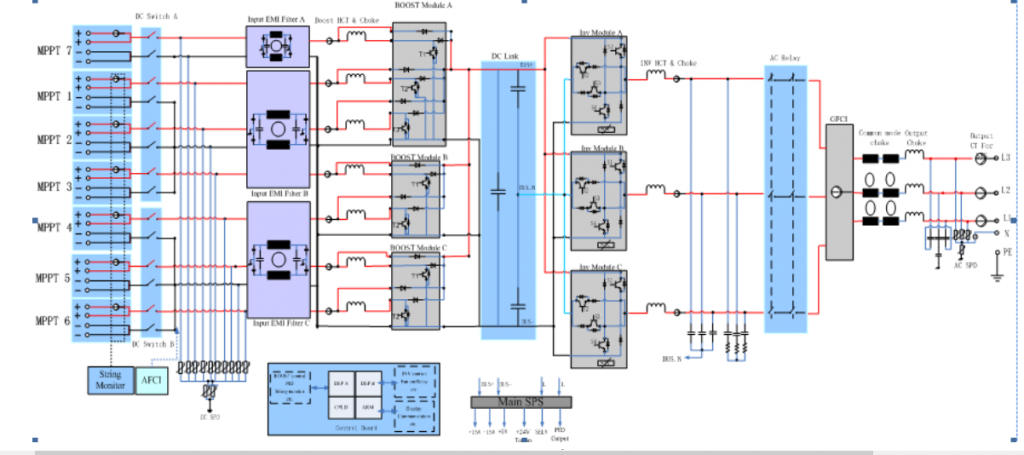
2. System Diagram
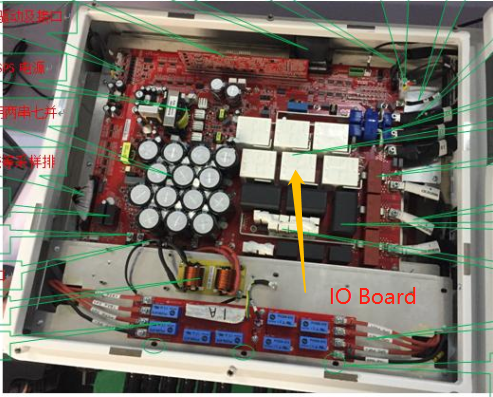
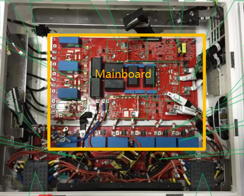
3. Board Introduction
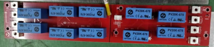
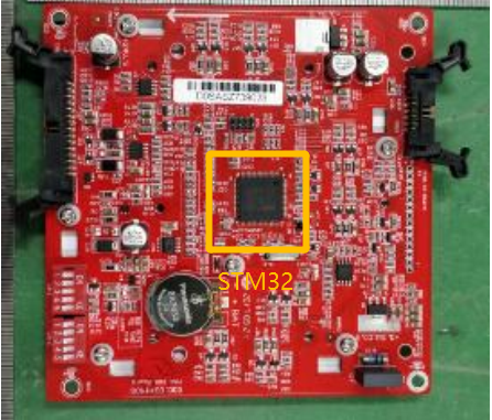
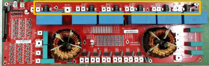
IO Board
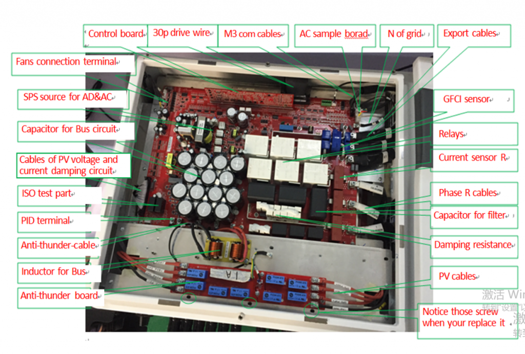
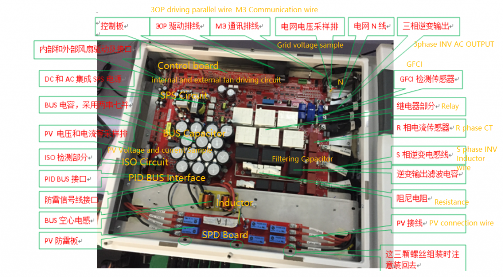
SPD Board
It is used to prevent lighting strike
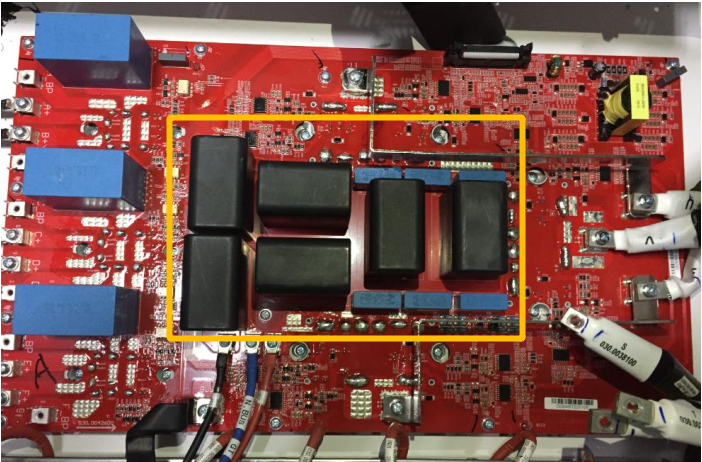
Inductor
It is used in BUS circuit and it is function is filtering wave
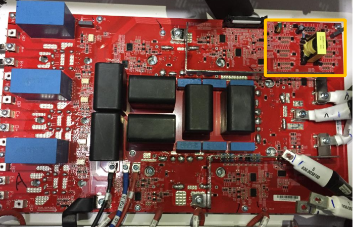
PID BUS Interface
PID means ” PotenTIal Induced DegradaTIon “, The direct harm of PID is that a large amount of charge accumulates on the surface of the cell, which deteriorates the passivation effect of the cell surface, resulting in a decrease in the fill factor, open-circuit voltage, and short-circuit current of the cell, and the power attenuation of the battery module.
SPS circuit
main SPS circuit
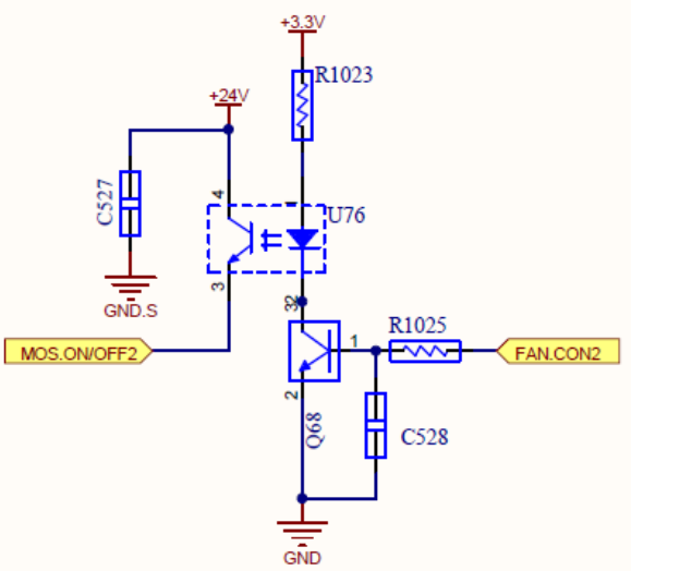
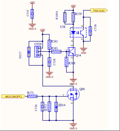
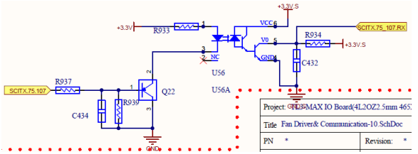
Internal and external fan driving circuit
3OP driving parallel wire
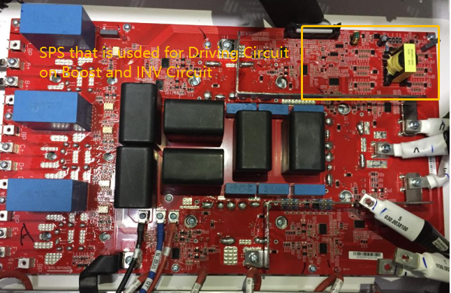
It is used to drive Boost and DC-AC circuit , SPS circuit on mainboard
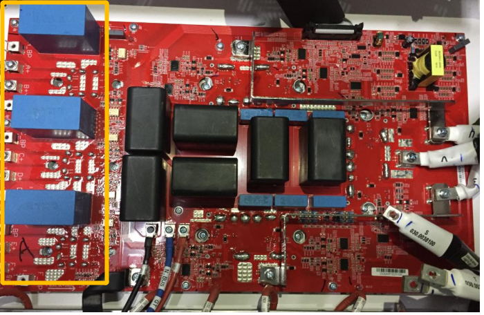
Resistance
It has been cancelled in new MAX series.
Left Cover of Max Inverter
Main board

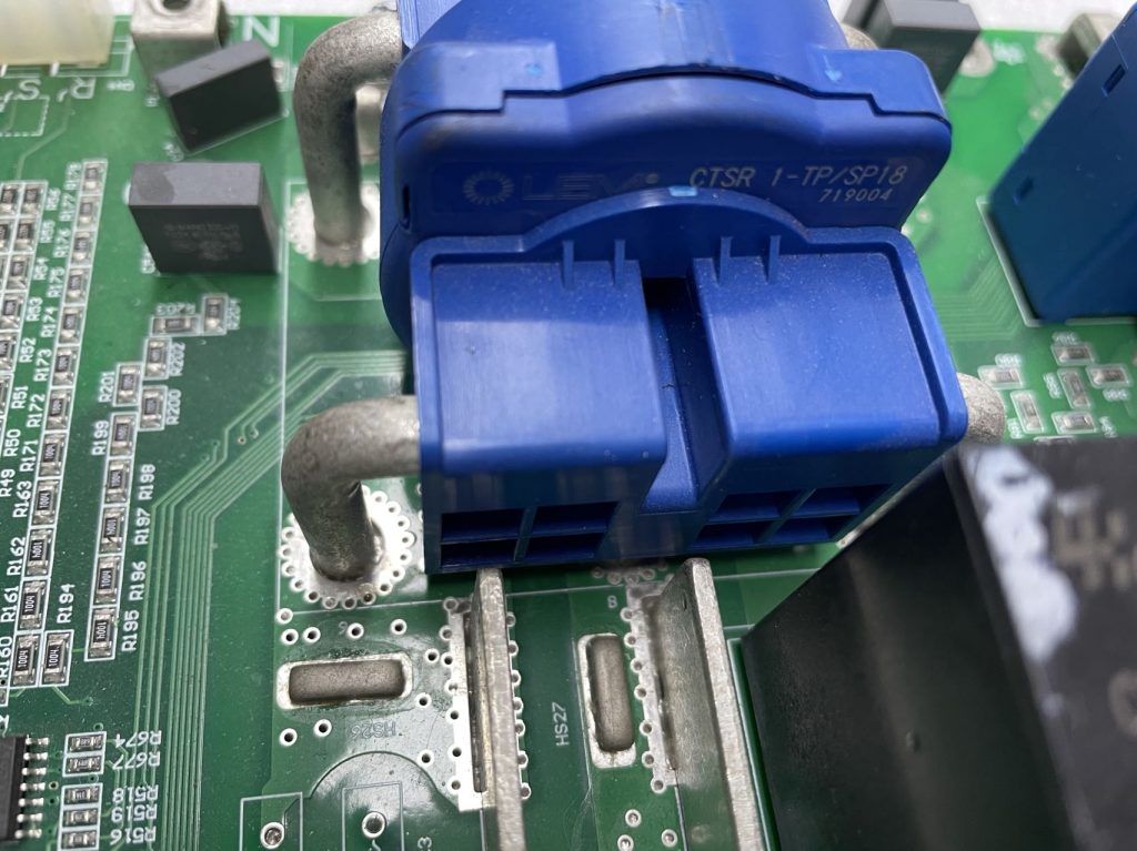
PV INPUT board
SPD board
Right Cover of Max Inverter
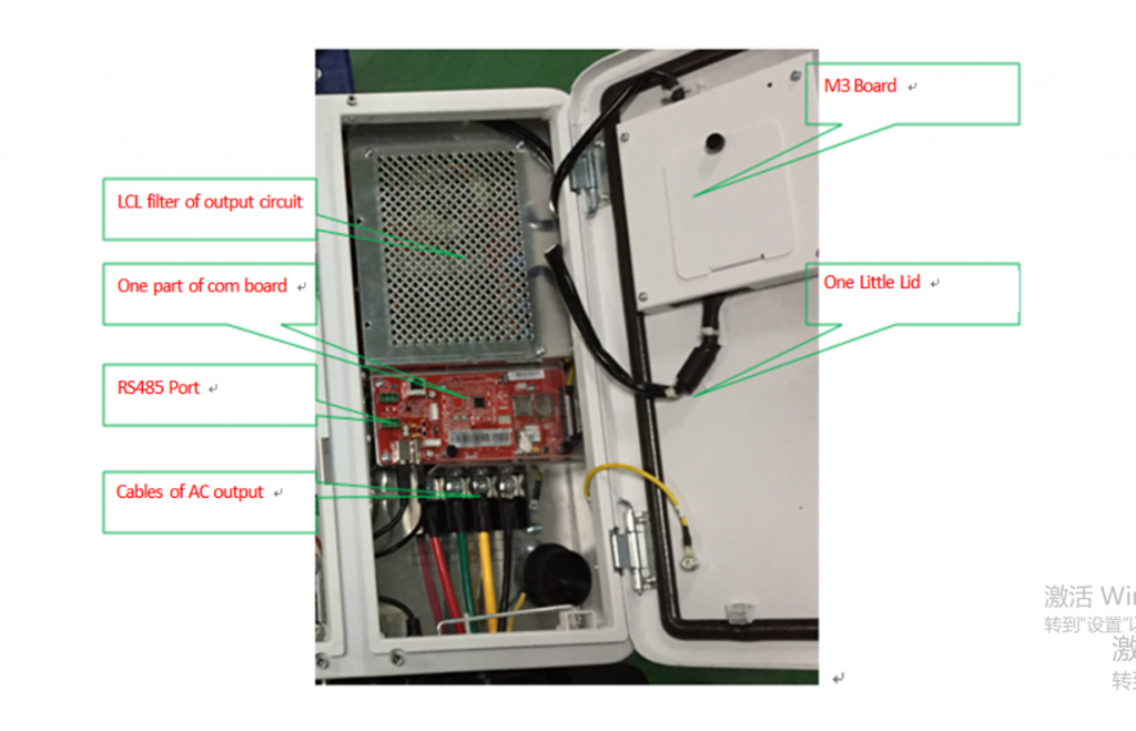
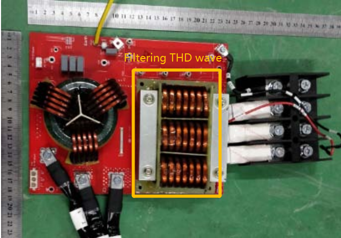
AC Filtering board
AC SPD board
M3 board
Control board
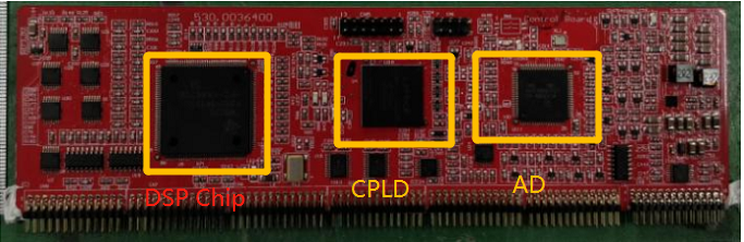
DSP Chip called 75 chip , Mainly deal with AC output Sampling data
AD chip called 67 chip, mainly deal with PV Sampling data
CPLD is used to produce wave and drive related circuit.
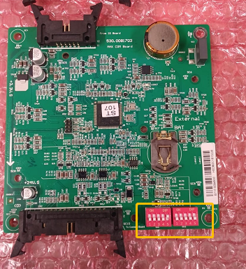
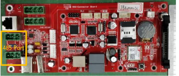
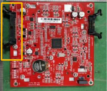
Communication Switch Board
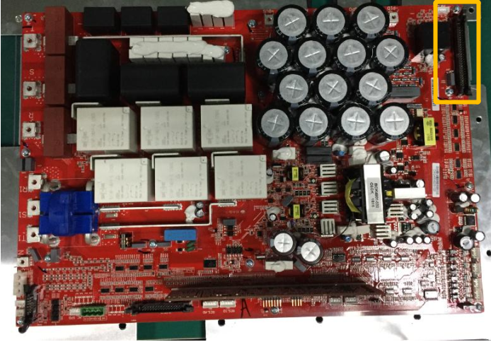
4. Board Position
5. Electrical Diagram Introdcution
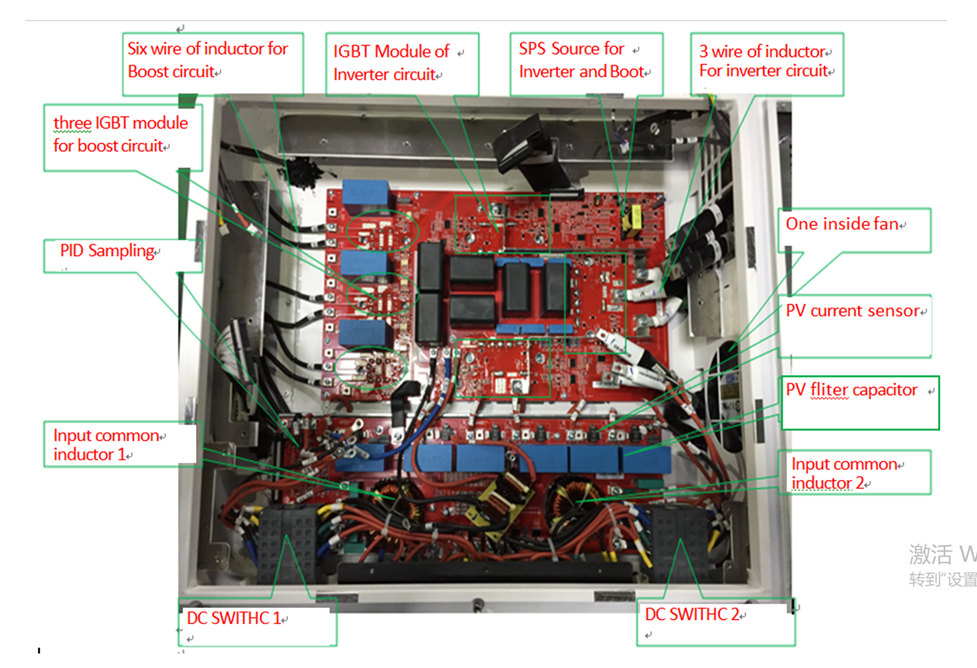
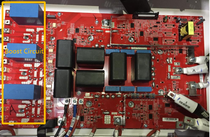
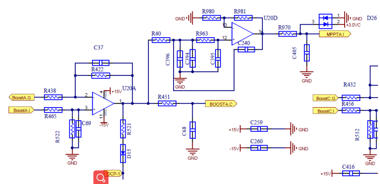
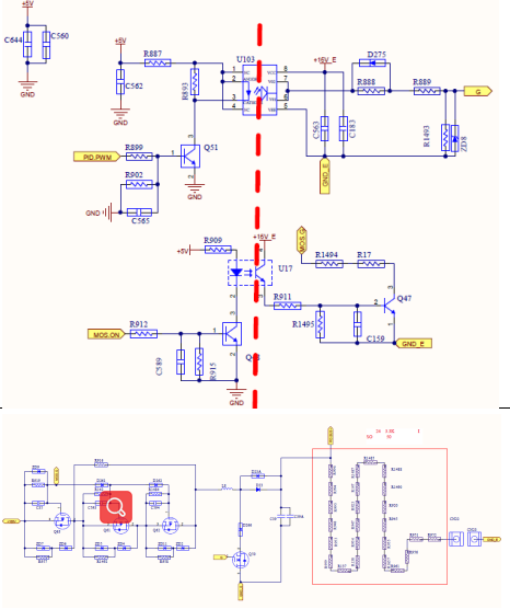
Boost Circuit on mainboard
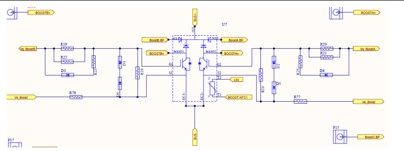
Driving circuit of Boost Circuit
BOOST. PWM1 is introduced into the main board from the control board through the 30PIN cable of the IO board, and outputs BoostA.PWM after passing through the optocoupler TLP352
As the driver of the BoostA. The other five are the same
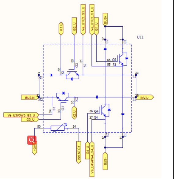
INV Driving Circuit

There are 12 routes in total on Inverter drive circuit, PWM through 8286 driver chip output Give to push-pull and then to Vge of IGBT
Full Bridge Circuit

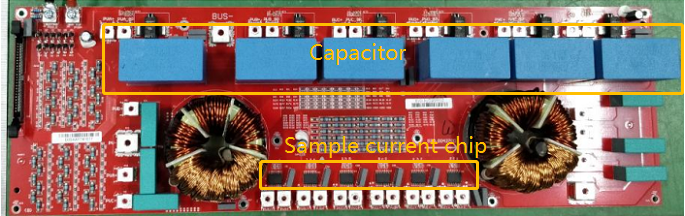
PV String Current Sampling Circuit
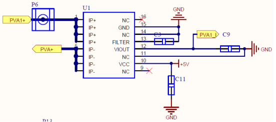

String current sampling circuit, the string current passes through the string chip and outputs the sampling voltage, and output of the sampling circuit to the operational amplifier
After scaling, it is given to the AD port of the control board to convert the current.
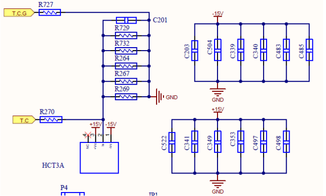
Boost Current Sampling Circuit
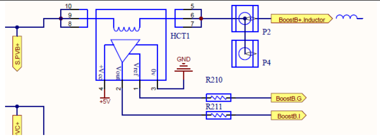
PV current through HCT (Current Sensing device) sampling, HCT voltage type, straightly Connect output sampling voltage. There are 6 routes in total
The PV current (BOOST inductor current) is sampled through the HCT. When a current flows through the HCT, the HCT itself outputs a sample signal. The sample voltage increases linearly (that is, the greater the current flowing, the greater the output voltage),
HCT output sampling After the voltage is transported After zooming to the control panel AD port to read Get real-time PV curren
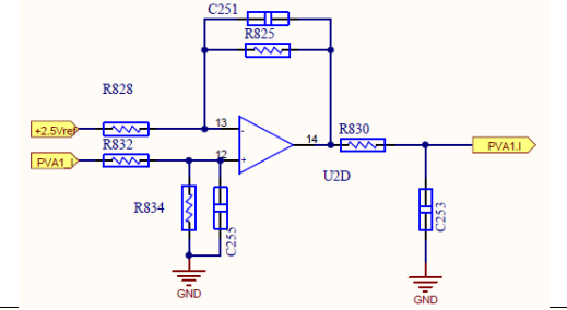
PV voltage Sampling Circuit
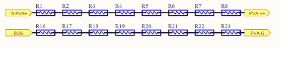
PVA road is the reference test, other five
the same way. Sampling resistor at PVinput
Board
stream to PVA as a reference, The other five Same.op on IO board.
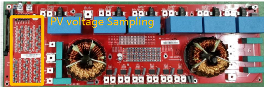
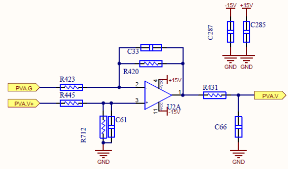
The PV voltage is divided by the resistor and sent to the op amp for scaling, and then sent to the control AD port for operation, so as to sample the PV Voltage.
BOOST OCP Protection Circuit
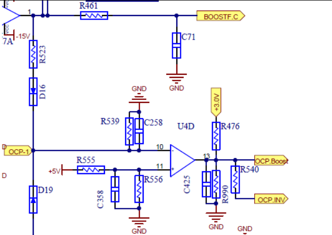
BOOST OCP Protection Circuit output voltage with an electron and diode via sampling current Op amp
Compare negative output of the comparator and positive voltage
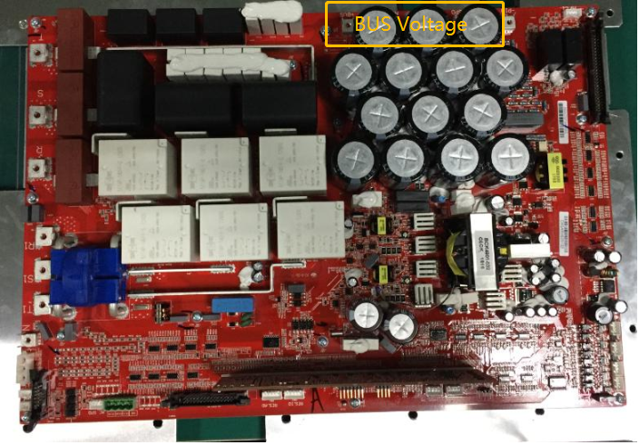
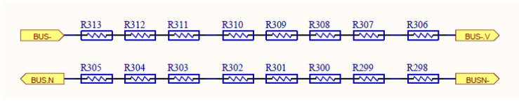
BUS Voltage Sampling Circuit
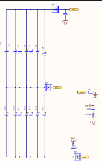
Negative BUS voltage Sampling Resistance
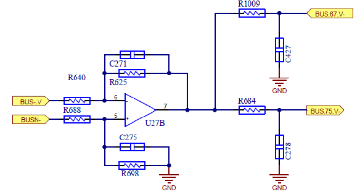
Negative BUS voltage Sampling op amp The output is divided into Second, give to 075 and 067 control chip
Positive BUS voltage Sampling Resistance
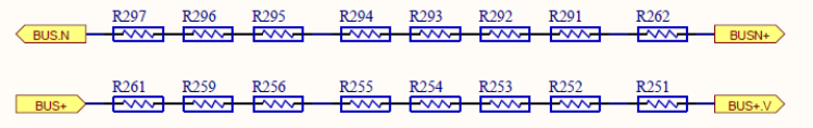
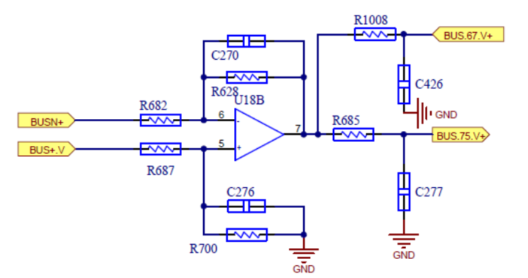
The total BUS voltage is summed by the positive and negative BUS voltages, and the positive and negative BUS voltages are sampled respectively, and then given by the op amp scaling.
The AD port of the control chip performs sampling and calculation to obtain the real-time voltage, and the output of the op amp is divided into two parts, which are respectively given to two different chips for sampling.
AC Current Sampling and OCP Protection Circuit
HCT Current Sensing sampler
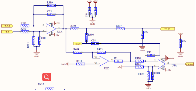
voltage to the op amp after zooming
is given to control
Board AD port.
OCP is made by
After the sample is taken out separately
given to the comparator
AC Voltage Detecting Circuit
Voltage sampling operation
output to
075 Chip
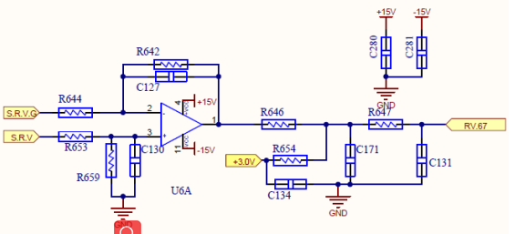
Voltage sampling operation
output to
067 Chip
The grid voltage is given to the op amp after being divided by the resistor, and then given to the control chip after scaling, and the two chips are sampled separately
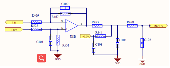
The inverter voltage is divided by the resistor and given to the op amp, and after scaling, it is given to the control board for sampling operation.
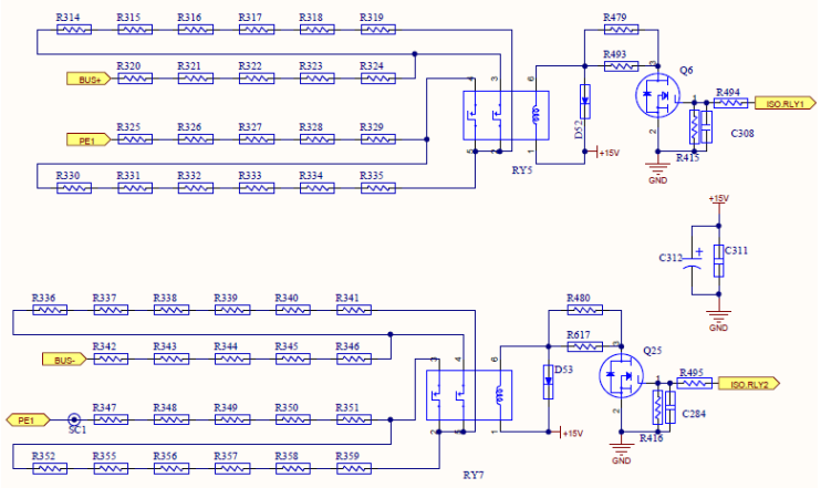
R phase Relay Circuit
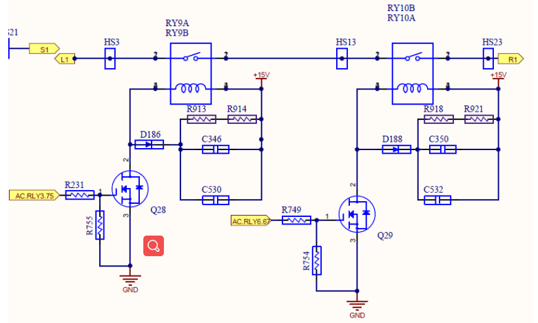

S phase Relay Circuit
T phase Relay Circuit

When it is about to be connected to the grid, the relay detection is carried out, and by switching the relay, and control INV Circuit to form wave., so that the inverter output and the grid Voltage at the same frequency and the same volt value, compare the voltage difference between the inverter side and the grid side to judge whether the relay can work normally
Detection logic:
1. Before the inverter produces the wave (before the relay driver works), detect the voltage across the inverter and the grid, if there is a large voltage difference 80V indicates that the first step has passed the test;
2. After the inverter produces the wave, firstly close the inverter relay to detect the voltage across the inverter and the grid.
If there is no voltage difference between the two ends, it means the relay on the grid side is stuck (or on the inverter side).
3. After the inverter produces the wave, firstly disconnect the inverter side relay, and then close the grid side relay to detect the power at both ends of the inverter and the grid. If there is no voltage difference between the two ends, it means that the inverter relay is stuck (the above inverter side is excluded at this time), otherwise there is a voltage difference and is greater than 80V
It means that there is no sticking;
4. At this time, close the relay on the inverter side again, and check the voltage across the inverter and the grid. If there is no voltage difference. It means that the detection is normal, and it is connected to the grid. Otherwise, there is a voltage difference and it is greater than 80V, which means that the relay cannot be closed.
Main SPS Circuit
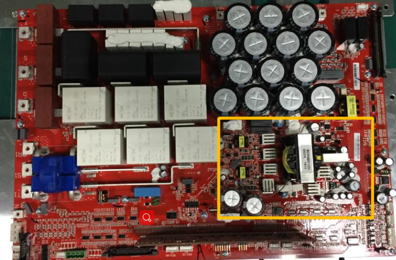
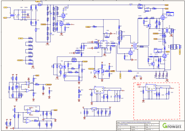
Auxiliary power SPS adopts integrated DC SPS and AC SPS, that is, DC SPS and AC SPS share a transformer,
The secondary side outputs are together, and the DC SPS takes power from the BUS, adopts an overlapping flyback topology circuit, and uses 2844 for the control driver chip;
The AC SPS takes power from the ST two-phase uncontrolled rectification, and also uses the overlapping flyback topology circuit, and the control driver chip also uses 2844.
The primary side of the transformer is controlled separately
DC SPS or AC SPS operation is performed by voltage judgment through comparator.
Input voltage range: PV =200-1100v, AC= 210v-615V
Output voltage range: +15V, -15v, 8V, 8v convert to 5V( 2567 Buck chip Degarde ),24V (Fans), 24V converted to 5V( 2567 Buck chip Degarde, for communication ), 100V( PID Input Voltage ), 15V(PID Driving Voltage)
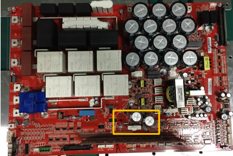
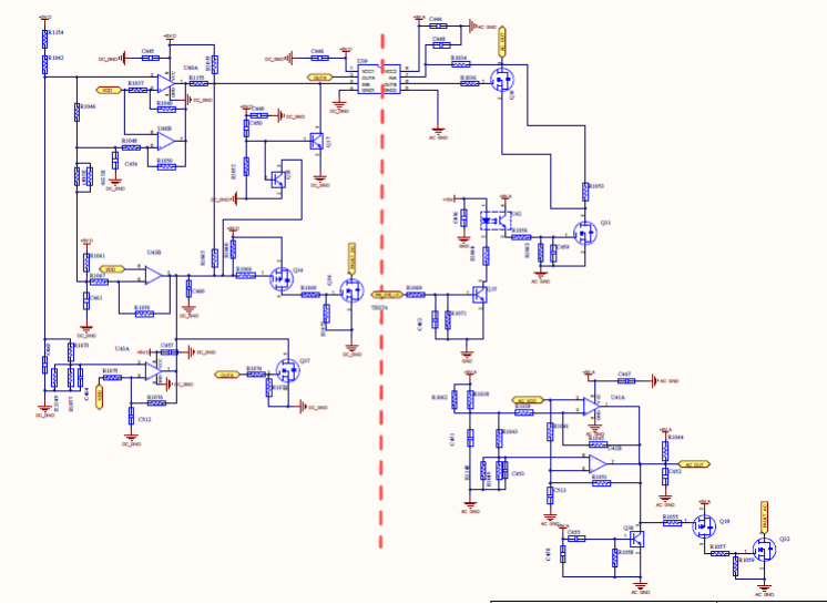
SPS Cirucuit on mainboard ( It is used for Boost and INV Driving Circuit)
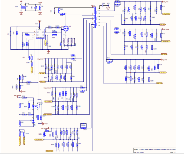
The BOOST drive voltage and inverter drive voltage of this model consist of an independent SPS. is a flyback topology, the control
chip is 2843, and there are 6 sets of outputs (the total output voltage of each channel is 22V, and then 15V is clamped by the Zener diode
and -7V. ), input 15V from main SPS output as power supply
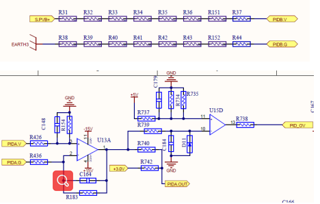
PID Circuit( Potential Induced Degradation )
PID working principle: It is to increase the voltage between PE ( ground) and PV+, and optimize the panel at night. actually
The topology of PID boosting is a BOOST circuit. After the main SPS outputs 100V, the voltage is boosted to the set voltage value.
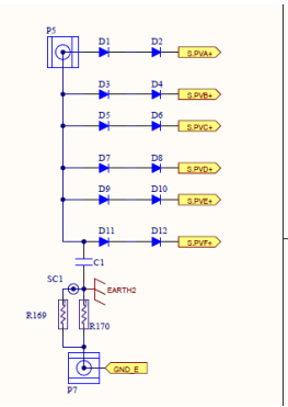
output, go
through the diode
directly after
PV input
positive electrode
FAN Circuit
GFCI Circuit (Ground Fault Circuit-Interrupter)
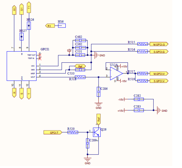
Principle: It is like RCD. When 3 phase in balance, current of Neutral line should be 0
Internal Communication Circuit (Between M3 board and control board)
Between 067 Chip on control board and M3 board
Between 075 Chip on control board and M3 board
ISO Circuit
The ISO detection circuit samples the voltage at both ends through the opening and closing of two relays, and then calculates the impedance between PV+ and PV- to PE. So as to determine whether it is OK.
30PIN Drive Row Wire
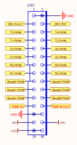
1,2 GND Control ground
3 DRV.Fault Driving fault alert
4 DRV.RST
5 T3.PWM T phase G3 IGBT Driving
6 T4.PWM T phase G4 IGBT Driving
7 T1.PWM T phase G1 IGBT Driving
8 T2.PWM T phase G2 IGBT Driving
9 S3.PWM S phase G3 IGBT Driving
10 S4.PWM S phase G4 IGBT Driving
11 S1.PWM S phase G1 IGBT Driving
12 S2.PWM S phase G2 IGBT Driving
13 R3.PWM R phase G3 IGBT Driving
14 R4.PWM R phase G4 IGBT Driving
15 R1.PWM R phase G1 IGBT Driving
16 R2.PWM R phase G2 IGBT Driving
17 BoostE.PWM BOOST E Driving
18 BoostF.PWM BOOST F Driving
19 BoostC.PWM BOOST C Driving
20 BoostD.PWM BOOST D Driving
21 BoostA.PWM BOOST D Driving
22 BoostB.PWM BOOST B Driving
23 TEMp.INV INV Temperature detecting
24 TEMp.BOOST BOOST Temperature detecting
25, 26 GND Control ground
27 +5V Main SPS power Supply
28 -15V Main SPS power Supply -15V
29.30 +15V Main SPS power supply +15V
50PIN Drive Row Wire
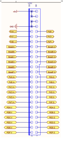
1、 2 pin:
PIDF.V PIDF.G
PID F Route Voltage Sampling
3、 4 pin:
PIDE.V PIDE.G
PID E Route Voltage Sampling
5、 6 pin:
PIDD.V PIDD.G
PID D Route Voltage Sampling
7、 8 pin:
PID C Route Voltage Sampling
9、10 pin:
PID B Route Voltage Sampling
11、12 pin:
PIDA.V PIDA.G
PID A Route Voltage Sampling
13、14 pin
PVF.V+ PVF.G
PV F Route Voltage Sampling
15、16 pin
PV E Route Voltage Sampling
17、18 pin
PVD.V+ PVD.G
PV D Route Voltage Sampling
19、20 pin
PVC.V+ PVC.G
PV C Route Voltage Sampling
21、22 pin
PVB.V+ PVB.G
PVB Route Voltage Sampling
23、24 pin
PVA.V+ PVA.G
PVA Route Voltage Sampling
25、26 pin
BoostF.I BoostF.G
PV F Route Inductor current Sampling
27、28 pin
BoostE.I BoostE.G
PVE Route inductor current Sampling
29、30 pin
BoostD.I BoostD.G
PV D Route inductor current Sampling
31、32 pin
BoostC.I BoostC.G
PV C Route Inductor Current Sampling
33、34 pin
BoostB.I BoostB.G
PV B Route Inductor Current Sampling
35、36 pin
BoostA.I BoostA.G
PV A Route Inductor Current Sampling
37 pin
PVF1_I
PVF Route String Current Sampling
38 pin
PVE1_I
PV E Route String Current Sampling
39 pin
PVD1_I
PVD String Current Sampling
40 pin
PVC1_I
PV C Route String Current Sampling
41 pin
PVB1_I
PVB Route String Current Sampling
42 pin
PVA1_I
PVA String Current Sampling
43、44、45、46 pin
GND
Control Ground
47、48、49、50 pin
+5V
Main SPS power supply +5V
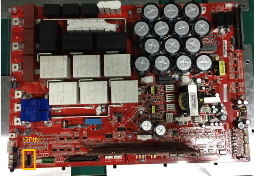
12 PIN Communication Row Wire
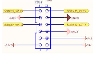
1 pin
+3.3V.S
SPS power supply +3.3V.S
2 pin
+24V
SPS power supply 24V
3、 4 pin
+5V.S
SPS power supply +5V.S
5、 6 pin
GND.S
Communication control ground
7 pin
SCITX.67_107.RX
067 sending data
8 pin
SCIRX.67_107.TX
067 receiving data
9 、10 pin
GND.S
Communication control ground
11 pin
SCITX.75_107.RX
075 sending data
12 pin
SCIRX.75_107.TX
075 receiving data
30 pin Communication row wire
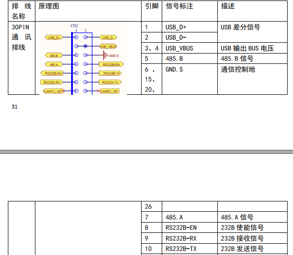
1,2 pin
USB D+ USB D-
USB differential signal
3,4 pin
USB_VBUS
USB output BUS voltage
5 pin
485.B
485.B Signal
6, 15, 20,26 pin
GND.S
Communication control ground
7 pin
485.A
485 A signal
8 pin
RS232B-EN
232B Enable signal
9 pin
RS232B-RX
232B Receiving signal
10 pin
RS232B-TX
232B Sending signal
11 pin
RS232.RX
232A Receiving data
12 pin
RS232A.TX
232A Sending data
13 pin
CANTX_107
CAN Sending signal
14 pin
CANRX_107
CAN Receiving data
16 pin
USB.ID
17、18 pin
+5V.S_OUT
Chip output 5V
19 pin
+3.3V.S
SPS power supply 3.3V.S
21-25 pin
27 pin
RE_IO3
28 pin
+24V.S
SPS power supply 24V.S
29 pin
RE_102
30 PIN
RE_101